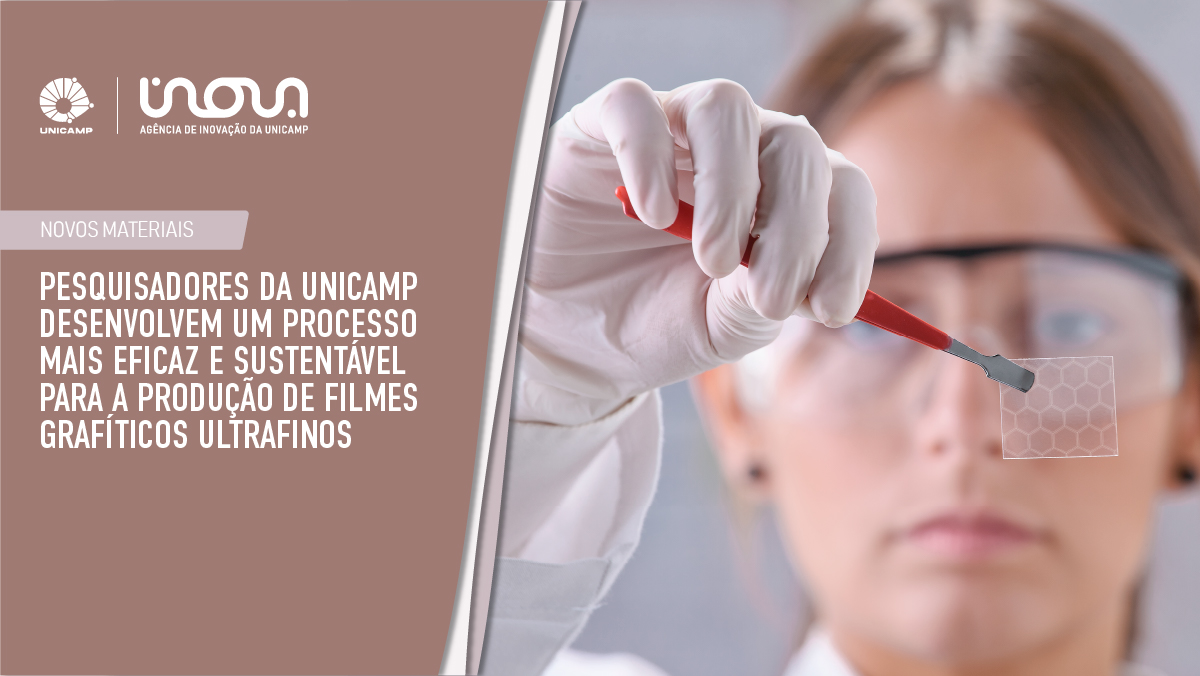
NOVELTY – Diamond-bearing magnetic film is made by using semiconductor material, magnetic material and microcrystalline or nanocrystalline by chemical vapor deposition. The magnetic material contains a paramagnetic metals, boron or sulfur. The chemical vapor deposition is performed by using metal, metal substrate or steel substrate and ethanol, water and boron at 1800-2400 degrees C for 1-100 hours. USE – Diamond-bearing magnetic film used in electronics devices such as disk drives, transistors and biomedical devices (all claimed). ADVANTAGE – The diamond-bearing magnetic film enables the calculation of computational data efficiently by electronics devices. DETAILED DESCRIPTION – An INDEPENDENT CLAIM is included for a method for developing diamond-bearing magnetic film, which involves dripping motor oil containing molybdenum disulfide near the filaments and pre-treating substrate with iron or steel and acetone.
L03 (Electro-(in)organic – chemical features of conductors, resistors, magnets, capacitors and switches, electric discharge lamps, semiconductor and other materials, batteries, accumulators and thermoelectric devices, including fuel cells, magnetic recording media, radiation emission devices, liquid crystals and basic electric elements. Growing of single crystals of semiconductors and their doping are included, but semiconductor devices, where the manufacture is not claimed are excluded. Electrography, electrophotography, magnetography, electrolysis, electrophoresis, power plant, X-ray and plasma-techniques, ion exchange resins, polyelectrolytes, electroplating, metal electrodeposition, electroforming, anodising, electrolytic cleaning, cathodic protection and electrolytic or electrothermic production or refining of metals are all covered elsewhere (Sections G, J, K and M).); U11 (Semiconductor Materials and Processes)